This document complements this other
one, discussing possible design procedures for a "double resonance
solid-state Tesla coil", but now considering a lossless system [1]. The
objective is to design the structure below, when the driving signal is
sinusoidal (or a square wave, since this narrow bandwidth system responds
essentially only to the fundamental harmonic), requiring that after a
certain number of cycles of the input all the energy in the network is
concentrated at the output capacitance Cb. This is then equivalent to a Tesla
coil, where functionality is achieved through the zero-state response of
the network, caused by the input voltage Vin, instead of by the zero-input
response of the classical system, caused by an initial voltage in Ca, with Vin = 0.
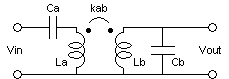
The design can be more easily done by first designing the transformerless structure below, and then converting it to the final structure through the relations shown. w0 is the "base frequency" in rad/s that multiplies k, l, and m (see below). The usual design would be to specify Ca, Cb, and Lb, and compute w0 and La from the equations. In all cases the coupling coefficient kab depends only on the "mode" k:l:m.
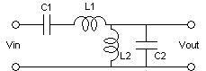
w02CbLb
= L2C2
w02CaLa
= C1(L1+L2)
kab = (L2/(L1+L2))1/2
The circuit is a 4th-order network with two resonance frequencies (pairs of poles at jw in the transfer function), and excitation is at a third frequency. I will assume that these three frequencies are in a ratio k:l:m or three positive integers. I will also consider initially a normalized design where the three frequencies are just k, l, and m rad/s (w0 = 1). Three possible designs that result in complete energy transfer can be identified:
a) The input signal is a cosinusoid, and the three
frequencies are in a ratio of successive integers with odd differences (as
1:2:3, or 10:11:14). The excitation is at the central frequency,
l. Complete energy transfer occurs in l/2 cycles of the
input. The required element values are:
C2 = 1
L2 = 1/l2
L1 = l2/((k2-l2)(l2-m2))
C1 = ((l2-m2)(k2-l2))/(k2m2)
b) The input signal is a sinusoid, and the three frequencies
are in a ratio of successive odd integers with double odd differences (as
1:3:5, or 21:23:29). The excitation is at the central frequency,
l. This is the most practical design.Complete energy transfer
occurs in l/4 cycles of the input. The element values are:
C2 = 1
L2 = (k-l+m)/(klm)
L1 = l(k-l+m)/((k-l)(k+m)2(l-m))
C1 = (l-m)(k+m)2(k-l)/(km(k-l+m)2)
c) The input signal is a sinusoid, and the three frequencies are in a ratio of successive odd integers with double odd differences, as in design (b). The excitation is at the upper frequency, m. This design is usually impractical, but listed here too. Complete energy transfer occurs in l/4 cycles of the input. The element values are:
C2 = 1
L2 = (k-l+m)/(klm)
L1 = -m(k-l+m)/((k-l)2(k+m)(l-m))
C1 = -(l-m)(k+m)(k-l)2/(kl(k-l+m)2)
There is no solution (with positive elements) for excitation at the lower
frequency, k.
The voltage gains (maximum Vout / peak Vin) for the three designs can be
calculated as:
a)Av = (Ca/Cb)1/2 2km/((k2-l2)(l2-m2))1/2
b)Av = (Ca/Cb)1/2 (km/((l-m)(k-l)))1/2
c)Av = (Ca/Cb)1/2 (kl/((k+m)(l-m)))1/2
When the multipliers k:l:m are successive (increasing by 2 in designs (b) and (c)), these expressions reduce to:
a) Mode k:k+1:k+2: Av = (Ca/Cb)1/2
k(k+2)/(4k2+8k+3)1/2
b) Mode: k:k+2:k+4: Av = (Ca/Cb)1/2
(k(k+4))1/2/2
c) Mode: k:k+2:k+4: Av = (Ca/Cb)1/2
k1/2/2
Designs (a) and (b) generate voltage gains approximately proportional to k. In design (c) the gain increases only with the square root of k.
Note that for these circuits there is always the possibility of driving
at one of the resonances, what produces a continuously growing output,
that ideally can result in any voltage gain. But the input current grows
too at the same rate. For given input and output capacitances, and output
inductance, The design procedures (a) and (b) above always reach a given
output voltage faster, and with smaller maximum input current. The only
problem is that the coupling coefficient may become too small (the voltage
gain is inversely proportional to it), and the bandwidth of the system too
small too, but the same problem occurs in a system driven at a resonance,
if the input must be kept for many cycles. The same idea can be extended
for higher-order networks [2].
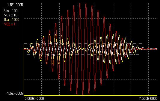
Examples:
Sinusoidal input, design (b) mode 11:13:15, Lb=30
mH,
Ca=10
nF, Cb=15
pF
Perfect energy transfer in 3.25 cycles.
Normalized transformerless circuit:
C1=
0.0969696970
L1=
0.0625000000
C2=
1.0000000000
L2=
0.0060606061
Final circuit:
Ca=
10.0000000000
nF
La=
49.3636363636
uH
Cb=
15.0000000000
pF
Lb=
30.0000000000
mH
kab=
0.2973176585
Output frequencies: 203172.34, 240112.77, 277053.19 Hz
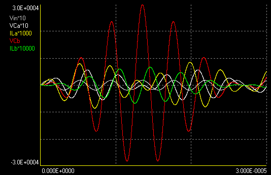
The waveforms above are for 180 V of input peak voltage. The predicted
voltage gain is 165.8312395178.
A simulation results in:
Maximum VCa
(V) = 571.69140 ( 0.00163 J) at 20.86709 us
Maximum ILa
(A) = 8.54905 ( 0.00180 J) at 19.84698 us
Maximum VCb
(V) = 29849.64157 (0.00668 J) at 13.53135 us
Maximum ILb
(A) = 0.67034 ( 0.00674 J) at 14.54545 us
Maximum voltage gain obtained = 165.83134
Ratio of maximum energies in the capacitors = 4.08927
Note that Ca and La must store only about 1/4 of the output energy. This happens in all practical cases.
It's also possible to design the system with irregular spacing of the three frequencies. If the mode is specified as 23:25:31 (double and add 1 (or -1) to k, l, and m, and then decrease l by 2), complete energy transfer occurs at a "second peak" of the transient waveform envelope, with a somewhat larger voltage gain.
Normalized transformerless circuit:
C1=
0.0583556942
L1=
0.0828760860
C2=
1.0000000000
L2=
0.0065077139
Final circuit:
Ca=
10.0000000000 nF
La=
36.0683367993 uH
Cb=
15.0000000000 pF
Lb=
30.0000000000 mH
kab=
0.2698266359
Calculated voltage gain= 199.0254031804
Maximum VCa
(V) = 642.53699 (0.00206 J) at 46.46265 us
Maximum ILa
(A) = 10.48317 (0.00198 J) at 45.50255 us
Maximum VCb
(V) = 35822.55794 (0.00962 J) at 26.12061 us
Maximum ILb
(A) = 0.80015 (0.00960 J) at 27.13471 us
Maximum voltage gain obtained = 199.01421
Ratio of maximum energies in the capacitors = 4.66239
If the central frequency is further approximated to one of the border
frequencies, the next solution produces a maximum at a "third peak", then
at a "fourth peak", and so on. These modes don't seem very practical,
however. In the example the output voltage increased by 20%, while the
maximum input current increased by 22.6%
A more practical design:
The previous designs didn't produce a high enough output voltage for a
spark producing coil. A more powerful system can be obtained by increasing
the primary capacitance and using a higher mode. Limiting the coupling
coefficient to 0.1, otherwise tuning becomes too critical, the highest
mode is 37:39:41 with design b. Complete energy transfer occurs in 9.75
cycles. To obtain 150 kV with 180 V square wave input (a half bridge
powered by the rectified 127 V power line, equivalent to 180*4/pi = 229
V), and using the same secondary coil and top load that I used in other
practical projects (Lb
= 28.2 mH, Cb = 10.4
pF), Ca has to be
increased to 12 nF. The final elements are then:
Ca=
12.0000000000 nF
La=
24.6977719183 uH
Cb=
10.4000000000 pF
Lb=
28.2000000000 mH
kab=
0.1021618888
Output frequencies: 279182.274741, 294273.208511 (excitation),
309364.142281 Hz
Created: 7 September 2004
Last update: 2 June 2020
Developed and Maintained by Antonio Carlos M. de Queiroz