This document describes some ideas that I had about the design of a "solid-state Tesla coil". This device, that is intended to produce effects similar to those of a classical capacitor-discharge Tesla coil, is basically an electronic inverter that switches a DC power supply over a network that resonates at the driver's frequency, converting the switched signal to a high-voltage output, producing sparks and "streamers", or radiofrequency corona. In this document I will concentrate on the design of the resonant network only, not discussing details of the electronic switcher. It is then a kind of Tesla coil that operates using the zero-state response of the network, instead of of the zero-input response as happens in a capacitor-discharge Tesla coil.
Low-pass L-match design
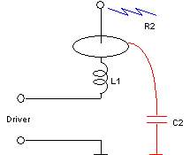
The most basic form for this kind of high-voltage generator is just a switcher and a resonant coil, as the secondary coil of a Tesla coil. A simple lumped model for this system is a driver connected to an inductor, with a load composed of a resistive load R2 and a capacitive load C2. I am initially considering the load as a parallel connection, although more correct would probably be to consider the existence of another capacitance in series with R2, since it represents "streamer loading" on the device. As the system operates essentially at a single frequency, however, this series circuit can be converted into an almost equivalent parallel circuit, and the capacitance associated with the streamers can be absorbed in C2. C2 is then the combination of the "self-capacitance" of L1, and the distributed capacitances of the device terminal, or top load, and of the streamers flowing into the air from it.
The resistive load for the actual devices is strongly nonlinear. In this linearized design, however, I am considering a nominal value for a linear R2, and centering the design around it. The result is a network that presents to the input a certain resistance R1 when the output load has a certain equivalent resistance R2.
It's desired to amplify the input voltage by a certain large voltage gain, and at the same time reflect a purely resistive impedance to the driver at the driving frequency. As the LC network is lossless, the input power must be equal to the power delivered to R2, and so the voltage gain is determined:
vin2/R1 = vout2/R2 => vout/vin = (R2/R1)1/2
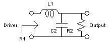
A possible approach for the design of this circuit is to consider L1-C2 as an "L-match" circuit converting R2 to R1. The design equations are then:
Q = (R2/R1-1)1/2
L1 = QR1/w0
C2 = Q/(w0R2)
Observe that the Q of the circuit is tied to the voltage gain, that for high gain must be high too, and that because of the high Q the circuit takes many cycles (about Q cycles) to reach the steady state. If R2 doesn't have the designed value, the input impedance doesn't remain resistive at the same driving frequency.
Example:
w0 = 2π300000 rad/s; vin = 200 V; vout = 50000 V; and R1 = 1 Ω, lead to:
R2/R1 = (50000/200)2 =
62500
Q = (62500-1)1/2 = 249.998
L1 = 132.628 mH
C2 = 2122 pF
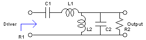
It's possible to design higher-order structures, still in this low-pass form, with series inductors and shunt capacitors. A simple approach is a cascade of two L-match networks, converting the resistance in two steps. The final element values may be more practical, and the time required for reaching steady state can be smaller. A more precise design is possible too, obtaining more control over the bandwidth and smaller sensitivity to changes in R2., by designing a filter that is like an even-order Chebyshev filter, but with the first attenuation maximum much smaller than the others. The design of this filter, however, is somewhat complicated.
Doubly terminated bandpass design
A more flexible and simple design can be obtained by using a transformer with both sides tuned. The design can be done as a bandpass Butterworth filter. Start with the specifications:
R = desired input resistance, ohms
w0 = Operating frequency in rad/s
B = 3 dB Bandwidth in rad/s
n = Voltage gain
Design a bandpass doubly terminated Butterworth (maximally flat) filter:
R1 = R2 = R
C1 = B/(w0221/2R)
L1 = 21/2R/B
L2 = BR/(w0221/2)
C2 = 21/2/(BR)
Convert it to the final structure:
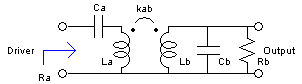
Ca = C1
La = L1+L2
Lb = n2L2
Cb = C2/n2
Rb = Rn2
kab = (L2/(L1+L2))1/2
Note that the relation L1C1 = L2C2 holds, but that (1-kab2)LaCa = LbCb. The driving frequency is the resonance frequency of the secondary circuit, but the primary circuit shall be tuned to a slightly lower frequency.
Example:
With 180 V of input voltage (a full bridge from 127 V rectified and
filtered) and peak current of 100 A, considering that the peak value of
the fundamental sinusoidal component of a square wave with 180 V of peak
value is 180(4/π)=229 V:
R = 2.29 Ω
With n = 500, operating frequency of 300 kHz, and a bandwidth of 50 kHz,
the final elements result as:
Ra: 2.29 Ω
Ca: 27.3 nF
La: 10.5 µH
Lb: 35.8 mH
kab: 0.117
Cb: 7.86 pF
Rb: 573 kOhms
The values are not very different from the usual for a capacitor discharge coil. This coil presents a constant resistance to the driver of 2.29 Ohms at 300 kHz, with little deviation for errors up to 25 kHz to each side. If the actual resistive load is different, the input impedance remains resistive, and the voltage gain doesn't change, because with both LC tanks tuned the system reduces to an ideal transformer with voltage gain n. This example results in two poles with Q = 8.5. The output voltage peaks at about this number of cycles, and stabilizes at 114.6 kV some cycles later. The input current has a similar behavior. The number of cycles required for output stabilization is a function of the bandwidth considered in the design. Larger bandwidths lead to faster stabilization.
The figure below shows a simulation of the output voltage and of the input current. The frequency response plots are in decibels, and so the output voltage at 300 kHz is shown as "101.2 dB", and the input current as "40 dB", corresponding to 114.6 kV and 100 A (peak values considered).
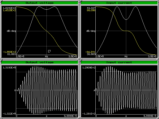
The frequency response gain is not flat around 300 kHz, because the output impedance of the driver was simulated as zero, while the design of the filter considered 2.29 Ohms. The input impedance, however, is "maximally resistive" around 300 kHz, as consequence of the design of the system as a doubly terminated LC filter. At the central frequency, the input reactance is zero, and the first two derivatives of the reactance in relation to the frequency are zero too, if the load resistance is as designed.
A measure of the energy available at the output is the energy stored at Cb at steady state.
E = (1/2)Cbvout2 = ((4/π)vin)2/(21/2BR)
where vin is the peak value of a square wave input. Noting that R = (4/π)vin/iin, where iin is the peak value of the input current, the required bandwidth for a given energy is obtained as:
B = (4/(21/2π))viniin/E
If Cb is specified, the voltage gain becomes determined:
n = π/vin(E/(8Cb))
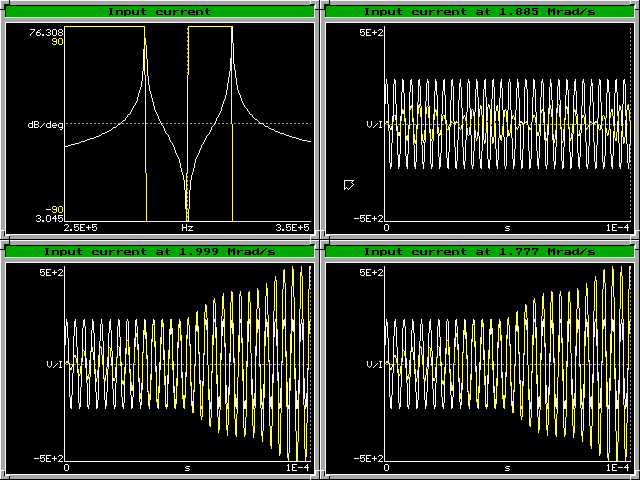
It is interesting to see what happens if the system is excited without load. The figure below shows what happens with the input current. The frequency response plot indicates that it goes to infinity at the resonances, and that the component at the driving frequency goes to zero at the central frequency. Excitation at the central frequency (1.885 Mrad/s) leads to regular beats caused by the two resonances, with periodical reversals of the direction of energy flow (the sinusoidal signal is the fundamental component of the input voltage). Excitation at the resonances (1.999 Mrad/s and 1.777 Mrad/s) result in continuous growth with beats, with continuous energy flow from the driver.
Singly terminated bandpass design
Another possibility is to design the filter with just one termination, what results in a maximally flat frequency response, but not in a maximally resistive input impedance. The formulas are:
R2 = R
C1 = B/(w0221/2R)
L1 = 21/2R/B
L2 = BR21/2/w02
C2 = 1/(BR21/2)
These values can be converted to the version with a transformer as in the first case. For the same specifications, the obtained values are:
Ca: 27.3 nF
La: 10.6 µH
Lb: 71.6 mH
kab: 0.164
Cb: 3.93 pF
Rb: 573 kΩ
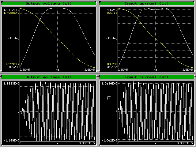
The values are not so convenient. Lb is too high, and Cb is too low (possibly irrealistic). The corresponding curves are below. Observe that the input impedance soon ceases to be resistive if the driving frequency is changed, as the phase curve departs quickly from zero degrees. The time-domain waveforms exhibit stabilization with smaller overshoot, corresponding to the behavior of a Butterworth filter.
If the output energy and Cb are specified, for this design the required bandwidth is obtained as:
B = (2/(21/2π))viniin/E
It is one half of the bandwidth for the doubly terminated case. For the same output energy, this design is twice slower in reaching the steady state. The voltage gain for a given Cb is the same of the doubly terminated case.
The formulas above can be rearranged for specified elements. For example, for given R, Ca, Cb and Lb:
Doubly terminated design:
La=LbCb/Ca+CaR2
w0=1/(LbCb)1/2
B=Ca21/2R/(LbCb)
kab=(B2/(2w02+B2))1/2=((CaR)2/(LbCb+(CaR)2))1/2
For the singly terminated design just La and kab are different, both larger:
La=LbCb/Ca+2CaR^2
kab=(B2/(w02+B2))1/2=((2CaR)2/(LbCb+2(CaR)2))1/2A different approach, considering a lossless system where the load is purely capacitive, is described here.
The program drsstcd can make these calculations and simulate the results.
Created: 19 June 2004
Last update: 25 May 2014
Developed and Maintained by Antonio Carlos M. de Queiroz