| Embedded Target for Motorola MPC555 |
  |
MIOS Pulse Width Modulation Out
Output driver for MIOS Pulse Width Modulation Submodule (MPWMSM)
Library
Embedded Target for Motorola MPC555
Description
The MIOS Pulse Width Modulation Out block is used for Pulse Width Modulation (PWM) output from the MIOS Pulse Width Modulation Submodule (MPWMSM). A PWM signal is a rectangular waveform whose period is constant but whose duty cycle can be varied, under control of a modulator signal, between 0% and 100%.
The MIOS Pulse Width Modulation block input signal acts as the modulator, controlling the duty cycle of the signal on the output pin. The input signal is constrained to be between 0 and 1. When the input signal value is 0, the output signal's duty cycle is 0%. When the input signal value is 1, the output signal's duty cycle is 100%.
There are two possible methods for calculating the period of the waveform. You can either control the scaling registers directly, or enter the desired (ideal) period and the mask will solve for the best values for the scaling registers.
Refer to section 15.12, "MIOS Pulse Width Modulation Submodule (MPWMSM)," in the MPC555 Users Manual for further information on the parameters described below.
Dialog Box
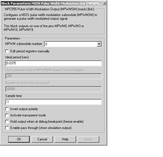
- MPWM submodule number
- Selects a PWM submodule for output.
- Edit period registers manually
- When this option is selected, the Clock prescaler field of MPWM Status/Control Register and Number of clock ticks per period edit fields are activated. You can then set the PWM period by setting these values.
- When this option is not selected, use the Ideal period (sec) field to set the PWM period parameters.
- Ideal period (sec)
- Specifies the desired period of the pulse signal. The mask then solves for the clock prescaler and the pulse period.
- Clock prescaler field of MPWM Status/Control Register
- Divides the counter clock to get the clock signal used to drive the PWM output. Note that the counter clock itself is derived from the MPC555 system clock as configured by the MPC555 Resource Configuration block (see MPC555 Resource Configuration).
- Number of clock ticks per period
- Determines the number of PWM counter ticks per pulse period. Valid values are
1 - 65535.
- Invert output polarity
- Switches the output level for logic one and zero.
- Activate transparent mode
- Bypasses the register double buffers. When transparent mode is active, a software write to the Next Pulse Width Register is immediately transferred to the Pulse Width Register. When transparent mode is inactive, the updated value only takes effect at the start of the next period.
- Hold output when at debug break point (freeze enable)
- Stops the PWM counters when a breakpoint is hit during debug mode, and holds the current output values.
- Enable pass through (show simulation input)
- Lets you provide a signal from this block for use in simulation. When this option is enabled, an outport appears on the block. The block input is passed through to the output during simulation. (See Data Type Support and Scaling for Device Driver Blocks for information on supported input/output data types and scaling of input/output signals.) Note that both the input and output signals are duty cycle values. This option affects simulation only.
| | MIOS Digital Out (MPWMSM) | | MIOS Waveform Measurement | |