| SimPowerSystems | |
Implement a universal three-phase bridge converter with selectable configuration and power switch type
Library
Description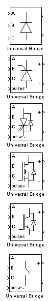
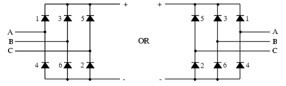
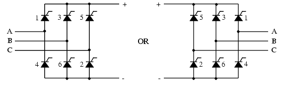
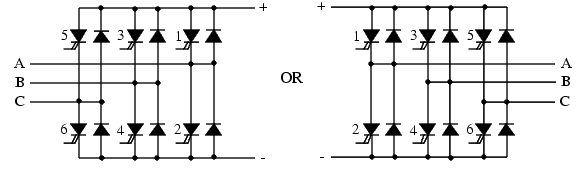
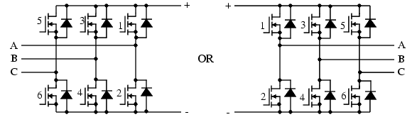
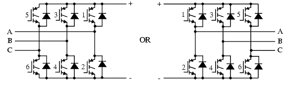
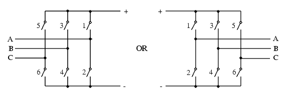
The Universal Bridge block implements a universal three-phase power converter that consists of six power switches connected as a bridge. The type of power switch and converter configuration are selectable from the dialog box.
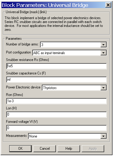
Dialog Box and Parameters
 ). Set the Snubber resistance Rs parameter to
 inf to eliminate the snubbers from the model. 0 to eliminate the snubbers, or to inf to get a resistive snubber.).| Measurement |
Label |
Inputs and Outputs
The bridge configuration is selectable so that the inputs and outputs depend on the configuration chosen:
Except for the case of a diode bridge, the Pulses input accepts a Simulink-compatible vectorized gating signal containing six pulse trains. The gating signals are sent to the power switches according to the number shown in the diagrams above.
Assumptions and Limitations
Universal Bridge blocks can be discretized to be used in a discrete time step simulation specified by the Discrete System block. In this case, the internal commutation logic of the Universal Bridge takes care of the commutation between the power switches and the diodes in the converter legs.
| Note In a converter built with individual forced-commutated power components (GTOs, MOSFETs, IGBTs), discretization of the model is not available. See Advanced Topics, for more details. |
Example
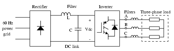
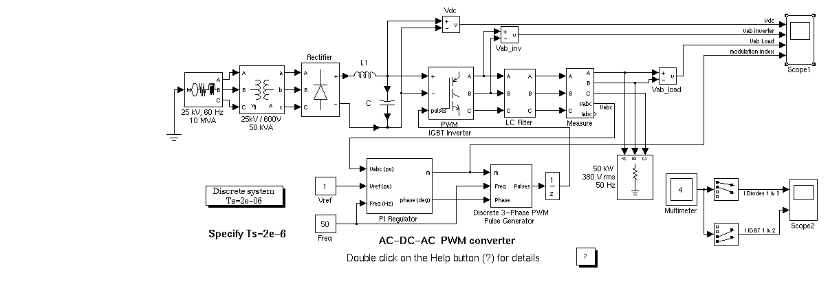
The psbbridges.mdl demo illustrates the use of two Universal Bridge blocks in an AC-AC converter consisting of a rectifier feeding an IGBT inverter through a DC link. The inverter is pulse-width modulated (PWM) to produce a three-phase variable-voltage variable-frequency sinusoidal voltage to the load. In this example the inverter chopping frequency is 2000 Hz and the modulation frequency is 50 Hz.
The IGBT inverter is controlled in a closed loop with a PI regulator in order to maintain a 1 p.u. voltage (380 Vrms, 50 Hz) at the load terminals.
A Multimeter block is used to observe commutation of currents between diodes 1 and 3 in the diode bridge and between IGBT/Diodes switches 1 and 2 in the IGBT bridge.
.The circuit is available in the demo.
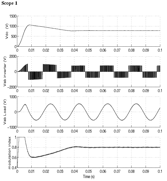
Start simulation. After a transient period of approximately 70 ms, the system reaches a steady state. Observe voltage waveforms at DC bus, inverter output, and load on Scope1. The harmonics generated by the inverter around multiples of 2 kHz are filtered by the LC filter. As expected the peak value of the load voltage is 537 V (380 V rms).
In steady state the mean value of the modulation index is m = 0.77, and the mean value of the DC voltage is 780 V. The fundamental component of 50 Hz voltage buried in the chopped inverter voltage is therefore
Vab = 780 V * 0.612 * 0.80 = 382 V rms
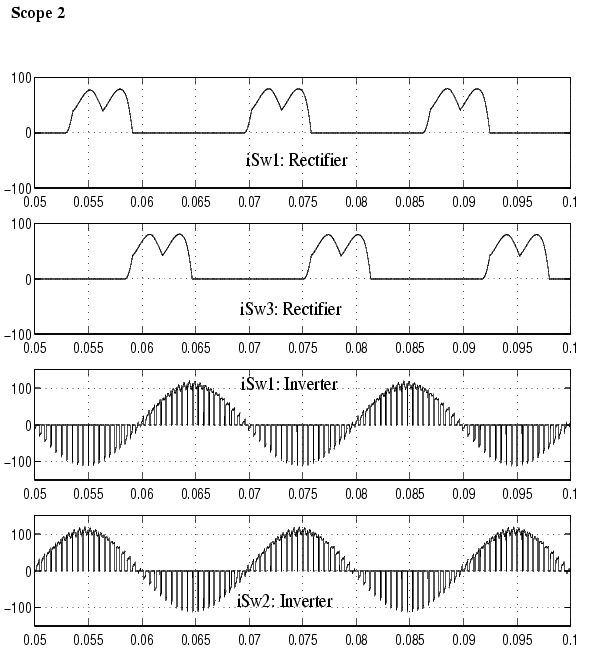
Observe diode currents on trace 1 of Scope2, showing commutation from diode 1 to diode 3. Also observe on trace 2 currents in switches 1 and 2 of the IGBT/Diode bridge (upper and lower switches connected to phase A). These two currents are complementary. A positive current indicates a current flowing in the IGBT, whereas a negative current indicates a current flowing in the antiparallel diode.
See Also
Diode, GTO, Ideal Switch, IGBT, MOSFET, Thyristor
| | Total Harmonic Distortion | Voltage Measurement | |