| SimPowerSystems | |
Implement a three-level neutral point clamped (NPC) power converter with selectable topologies and power switching devices
Library
Description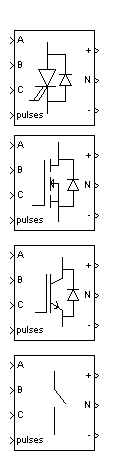
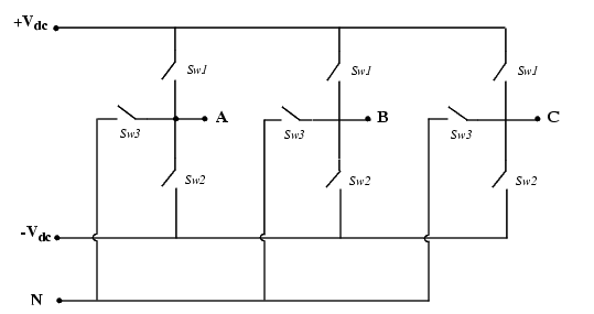
The Three Level Bridge block implements a three-level power converter that consists of one, two, or three arms of power switching devices. Each arm consists of four switching devices (Q1 to Q4) along with their antiparallel diodes (D1 to D4) and two neutral clamping diodes (D5 and D6) as shown.
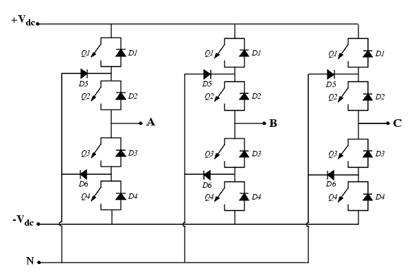
The type of power switching devices (IGBT, GTO, MOSFET, or ideal switch) and the number of arms (one, two, or three) are selectable from the dialog box. When the ideal switch is used as the switching device, the Three-Level Bridge block implements an ideal switch bridge having a three-level topology as shown.
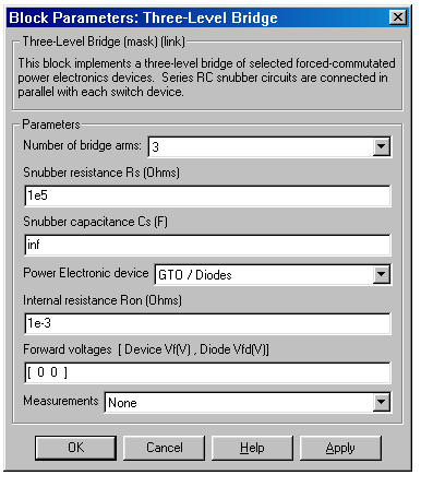
Dialog Box and Parameters
 ). Set the Snubber resistance Rs parameter to
 inf to eliminate the snubbers from the model. 0 to eliminate the snubbers, or to inf to get a resistive snubber.
 ).
).| Measurement |
Label |
device currents |
|
Inputs and Outputs
The bridge configuration is selectable, and the inputs and outputs depend on the configuration chosen:
The Pulses input accepts a Simulink-compatible vectorized gating signal containing four pulses (Q1 to Q4) for each leg of the converter. For instance, if a three-leg topology is selected, the input vector must contain twelve pulses and the ordering must be as follows: Q1 of leg A, Q2 of leg A, ..., Q4 of leg C.
| Note In the case of the ideal switch converter, Q1 pulse is sent to Sw1, Q4 pulse to Sw2, and a logical AND operation is performed on Q2 and Q3 pulses and the result sent to Sw3. |
Assumptions and Limitations
Turn-on and turnoff times (Fall time, Tail time) of power switching devices are not modeled in the Three-Level Bridge block.
Example
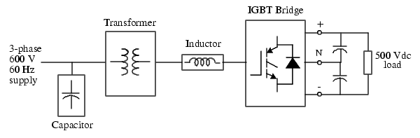
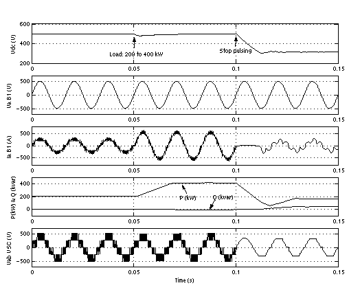
The psb3levelVSC.mdl demo illustrates the use of the Three Level Bridge block in an AC-DC converter consisting of a three-phase IGBT-based voltage sourced converter (VSC). The converter is pulse-width modulated (PWM) to produce a 500 DC voltage (+/- 250V). In this example the converter chopping frequency is 1620 Hz and the power system frequency is 60 Hz.
The VSC is controlled in a closed loop by two PI regulators in order to maintain a DC voltage of 500 V at the load while maintaining a unity input power factor for the AC supply.
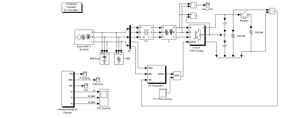
The initial conditions for a steady state simulation are generated by running an initial simulation to steady-state for an integer number of cycles of 60 Hz. The final states (both Power System Blockset and Simulink controller states) are saved in a vector called xInitial. This vector, as well as the sample times (Ts_Power and Ts_Control) are saved in the psb3levelVSC_xinit.mat file.
Load the initial condition MAT file and start the simulation. Observe the following signals:
At 50 ms, a 200-kW load is switched in. You can see that the dynamic response of the DC regulator to the sudden load variation from 200 kW to 400 kW is satisfactory. The DC voltage reverts to 500 V within 2 cycles and the unity power factor on the AC side is maintained.
At 100 ms, a Stop Pulsing signal is activated and the pulses normally sent to the converter are blocked. You can see that the DC voltage drops to 315 V. A drastic change in the primary current waveform can also be observed. When the pulses are blocked, the Three-Level Bridge block operation becomes similar to a three-phase diode bridge.
The following two figures summarize the results of the simulation. The first figure shows the operation of the AC-DC converter during the load variation and when the pulses are blocked.
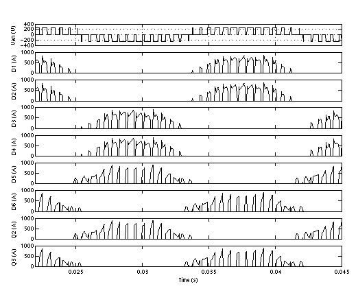
The second figure shows the current flowing in the various devices of the IGBT bridge when the converter is feeding 500 Vdc to a 200-kW load.
| | 3-Phase Sequence Analyzer | Three-Phase Transformer (Two Windings) | |